SEM imaging
What is SEM Imaging?
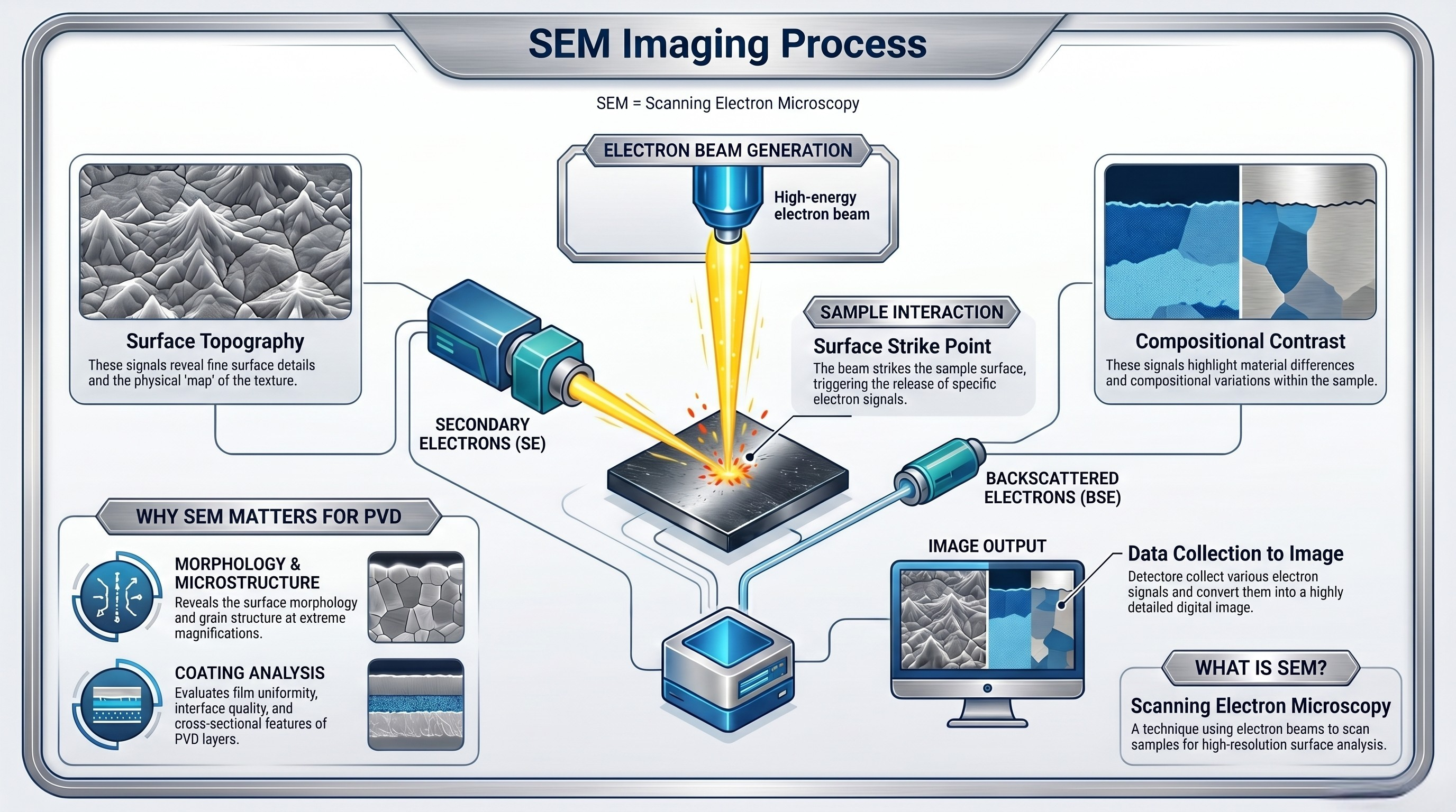
SEM, or Scanning Electron Microscopy, is a technique used to observe the surface structure and microstructure of a material at very high magnification. Instead of using visible light like a traditional optical microscope, SEM uses a focused electron beam to scan the surface of the sample and generate highly detailed images.
How SEM Works
When the electron beam strikes the sample surface, it interacts with the material and produces different signals, including secondary electrons and backscattered electrons. These signals are collected by detectors and converted into an image. Secondary electrons are commonly used to show surface topography and fine detail, while backscattered electrons can help reveal differences in material composition and contrast.
SEM Imaging Workflow
Why It Matters
SEM is an important tool for examining coating surfaces, cross-sections, and microstructural features that cannot be seen with the naked eye or with standard optical inspection. It provides high magnification, strong depth of field, and clear imaging, making it useful for analyzing surface condition, coating structure, and interface quality.
How It Supports PVD Quality Control
In PVD applications, SEM imaging can be used to observe coating morphology, film uniformity, and cross-sectional structure. It can also help evaluate the interface between the coating and the base material, supporting a better understanding of coating quality, thickness consistency, and adhesion-related characteristics. When combined with EDS analysis, SEM can provide even more information about localized material composition.
Case Example
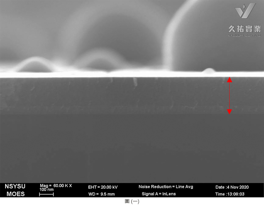
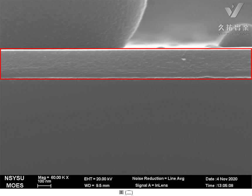
The SEM image below shows a magnified cross-sectional view of a coated sample. Figure (1) shows an image magnified 60,000 times, with the observed area indicated by the red arrow. In Figure (2), the area marked by the red frame shows a cross-sectional test view, revealing a uniform inlaid film and a solid film layer. This type of analysis helps evaluate coating structure, film uniformity, and interface quality at high magnification.